
FreePDK15:Analog Artist with HSPICE
This tutorial will introduce you to the Cadence Environment: specifically Composer, Analog Artist and the Results Browser. It will also show you how to use the simulator HSPICE in stand-alone mode to make certain parts of your design exploration easier.
ECE 546Students:
This tutorial is currently under construction. It is designed to introduce you to the tools we will use in class.
Proficient use of Cadence and Hspice will allow you to complete the projects and homework quickly, and will make the class more fun. Practice is really the only way to achieve such proficiency. There are probably an infinite number of tricks and short-cuts to make the design process easier, or at least enough to fill a small book. No tricks or short-cuts are covered in this tutorial and it will be up to you learn more about the tool and how you can use it better for your needs.
Lastly, the screen-shots in this tutorial may vary slightly from what you will see. Refer to the text next to the screen-shot for up-to-date information. Note also that some screen-shots have been shrunk to make the page more readable. In this case, please click on the image to view its wiki-page, and click on the image again to download the full-size image.
Contents
[hide]
- 1 Create Aliases to Setup Your Environment
- 2 Start the Cadence Design Framework
- 3 Create the myInverter Schematic
- 4 Create Input and Output Pins
- 5 Create Symbol from Cellview
- 6 Simulate the Schematic with HSPICE within Analog Artist
- 6.1 Set up the Simulation Environment
- 6.2 Choose a Simulator
- 6.3 Setting Up the Simulator
- 6.4 Generate the HSPICE Netlist
- 6.5 Saving the HSPICE Netlist
- 6.6 Running the HSPICE Netlist
- 6.7 Viewing your waveform
- 6.8 Saving ADE L State
- 6.9 Archiving the Project Folder for upload evaluation
- 6.10 Navigating the Hierarchy
- 6.11 DC Simulation
Create Aliases to Setup Your Environment
First of all, you should know that there is another Tutorial that goes through the shortcut/binding keys for Cadence. Please refer to this if you are having trouble finding a menu item to use in all tutorials.
Before you start this tutorial, add the following line to the .mybashrc file in your home directory:
alias setup_freepdk15=’source /mnt/designkits/ncsu/FreePDK15/cdslib/setup/setup.sh’
The line defines an alias that gives a command to setup your environment to use the FreePDK15 design-kit with the Cadence tools.
Before moving on, either source your .mybashrc file or log out and log back in.
Note to users outside NCSU:
The scripts mentioned above is provided in $PDK_DIR/cdslib/setup/setup.sh.
Start the Cadence Design Framework
- Log in to a Linux machine. The setup for this tutorial is currently supported only on Linux machines.
- Create a directory to run this tutorial, called something like “adetut” (for Analog Design Environment Tutorial). Change to this directory.
- Type module load synopsys/2021 ic/6.18-270 and this should load Synopsys HSPICE, Cadence
- Type “setup_freepdk15” at the command prompt. This will setup your directory by copying in various files that are needed to run the Cadence tools, including .cdsinit, lib.defs, and cds.lib. It will also define environment variables needed by the HSPICE libraries.
- Start the Cadence Design Framework by typing “virtuoso &” at the command prompt.
NOTE 1: you want to make sure that you do not have an INITIAL .cdsinit file in this folder. If you do, make a backup of it before running the setup_freepdk15 to .cdsinitold so that the script will copy the new one to your directory. you can check this by typing ls .cdsinit and see if it gives you any files.
NOTE 2: if you see a ece% sign for your command prompt, then you will want to type bash and then press return.
NOTE 3: Presently, some people have an issue running in the EBII 1028 computer lab on the RHEL8 machines. You MAY need to log into the remote computer cluster with RHEL7 if you are having issues on RHEL8. These problems show themselves as unable to save or write to files such as cds.lib file. To run in the 1028 computer lab if you are having these issues do ssh -X grendel and log in. The X windows will be shown on your local space and you will be running on the grendel server cluster and avoid the issues.
$ mkdir adetut
$ cd adetut
$ setup_freepdk15
$ module load synopsys/2021 ic/6.18-270
$ virtuoso &
The first window that appears is called the CIW (Command Interpreter Window).
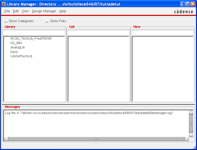
Another window that is very handy is the Library Manager, which allows you to browse the available libraries and create your own. To display this window, choose Tools -> Library Manager… from the CIW Menu.
Create the myInverter Schematic
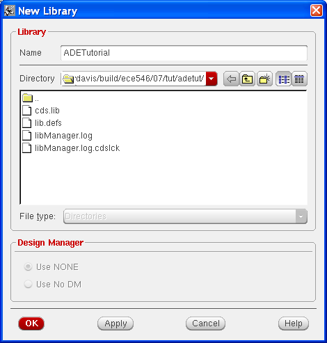
In the Library Manager, create new library called ADETutorial. Select File->New->Library. This will open new dialog window, in which you need to enter the name and directory for your library. By default, the library will be created in the current directory. After you fill out the form, it should look something like this:
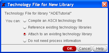
Click OK. Next, you will see a window asking you what technology you would like to attach to this library. Select “Attach to an existing technology library” and click OK. In the next window, select “NCSU_TechLib_FreePDK15”.

You should see the library “ADETutorial” appear in the Library Manager.

Next, select the library you just created in the Library Manager and select File->New->Cell View…. We will create a schematic view of an inverter cell. Simply type in “myInverter” under cell-name and “schematic” under view. Click OK or hit “Enter”. Note that the “Application” is automatically set to “Schematics L”, the schematic editor.
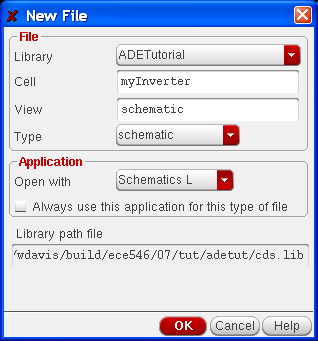
Alternatively, you can select the “Schematics L” tool, instead of typing out the view name. This will automatically set the view name to “schematic”.
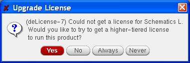
Click Ok. You may see the following window. Simply click “Yes” or “Always” to ignore this warning.
After you hit “Yes” or “Always”, the blank Composer screen will appear. The image below shows the final schematic that we will make in this tutorial.

The help manuals for Schematics are found here:
To generate a schematic like this, you will need to go through the following steps:
From the Schematic Window, choose Create->Instance…. The Add Instance, dialog will appear.
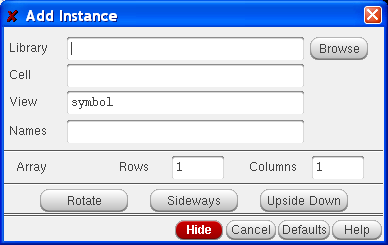
We will place the following instances in the Schematic Window as instructed below:
Description Library Cell View NMOS Transistor NCSU_TechLib_FreePDK15 nmos symbol PMOS Transistor NCSU_TechLib_FreePDK15 pmos symbol Supply Nets analogLib vdd, gnd symbol Voltage_Sources analogLib vdc, vpulse symbol Passive Elements analogLib cap symbol
Note: pay special attention to the parameters specified in vdc, vpulse, and cap. These parameters are very important in simulation.
Place pmos instance
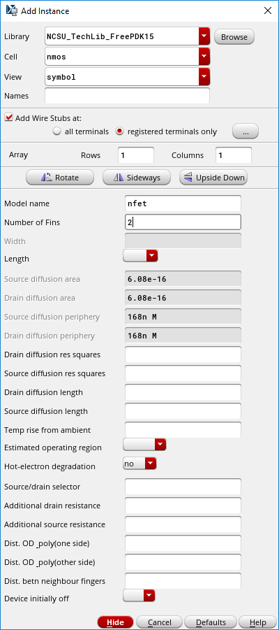
In the Add Instance (shortcut should be the letter i) window, select the pmos cell from the library NCSU_TechLib_FreePDK15. You may either type the values in or click Browse and find them in the Library Manager. After you select the cell, the “Add Instance” dialog will change to show the options for this cell. Note that most parameters are filled in automatically. The most important one for our purposes is “Number of Fins”, which is set to 2 by default. The “Width” and “Length” fields are left blank, because they are not needed by the BSIM-CMG transistor model that we will be using. Place the PMOS cell in the Schematic Window

Place nmos instance
Next, in the Add Instance window, select the nmos cell from the library NCSU_TechLib_FreePDK15. Ensure that “Number of Fins” is set to 2. Place the cell in the Schematic Window
Place gnd and vdd instances
Next, from the analogLib library, place intances of gnd and vdd in the Schematic Window.
Place wires for Gates, Bulk, and Source
- In the Schematic Window menu, select Create -> Wire (narrow)
- Place the wire to connect the input and bulk to source nodes as in the image below
- Select File -> Check and Save.

Create Input and Output Pins
Create Wires as you go for connecting input and output.
Next, you need to create two pins. One for input and one for output. Press the create Create Pin icon on the tool bar (shortcut should be the letter p).
Label the Pin I and the type to input and Place the pin in the Schematic Window

Label the next Pin O and the type to input and Place the pin in the Schematic Window

You do not need to make pins for power and ground in here. They are “globals” when defined this way and will automatically get passed down into the schematic.

Create Symbol from Cellview
From the Schematic Window select Create->Cellview->From Cellview…

Cellview Crom Cellview window appears. Make sure thew view name is symbol. Press OK.

Symbol Generation Options window appears. Left pins (inputs) should be I and right Pins (outputs) should be O. Press OK.

Symbol Editor window should now appear with a default square symbol.

Modify the symbol to represent an inverter like below.

Create Inverter Test Bench
You are going to create a new schematic just as you created the one for myInverter except this time you will call it myInverterTestBench.
Go back to the Library Manager and create a new blank cellview for myInverterTestBench in the ADETutorial Library.
Once here place an instance (shortcut i or from the menu tool bar).
From the ADETutorial library, select myInverter symbol. Place it in the Schematic Window.

Place vdc instance
You are now going to place the sources and capacitors in the test bench Schematic Window like below:
Next, from the analogLib library, select vdc symbol. In the DC voltage field, enter VDD_VAL. Note that the “V” will be inserted automatically. Place it in the Schematic Window. This will parameterize the VDD value to be used in later simulations.

Place vpulse instance
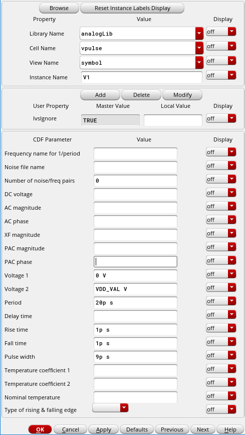
Next, from the analogLib library, select vpulse symbol. Enter the following values in the form:
Voltage 1: 0 V Volrage 2: VDD_VAL V Delay Time: 0 s Rise Time: 1p s Fall Time: 1p s Pulse Width: 9p s Period: 20p s
Place it in the Schematic Window.
Place cap instance
Next, from the analogLib library, select cap symbol. Enter “1f” in the Capacitance field. Note that the “F” will be filled in automatically. Place the instance in the Schematic Window.

Place OUT pin
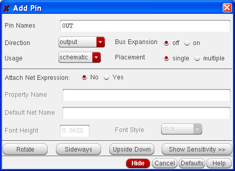
- From the Schematic Window menu, select Create -> Pin…
- In the Pin Names field , enter OUT
- In the Direction field, select output
- Place it in the Schematic Window
Place wires
- In the Schematic Window menu, select Create -> Wire (narrow)
- Place the wire to connect all the instances
- Select File -> Check and Save.
Also, it might be a good time to label nodes that are unlabeled for ease of simulation and viewing. You can do this by from the toolbar for label or by pressing the l and then setting the name. Notice in the tutorial this has been done for the IN node in the testbench.
Look at the CIW. You should see a message that says:
Extracting "myInverter schematic"
Schematic check completed with no errors.
"ADETutorial myInverter schematic" saved
If you do have some errors or warnings, the CIW will give a short explanation of what those errors are. Errors will also be marked on the schematic with a yellow or white box. Errors must be fixed for your circuit to simulate properly. When you find a warning, it is up to you to decide if you should fix it or not. The most common warnings occur when there is a floating node or when there are wires that cross but are not connected. Just be sure that you know what effect each of these warning will have on your circuit when you simulate.
Your schematic should look like the one shown below.
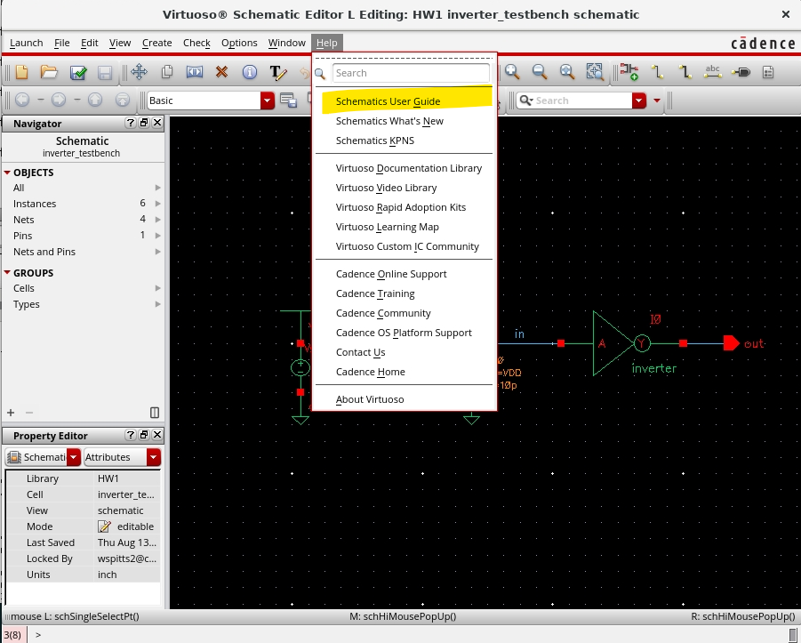
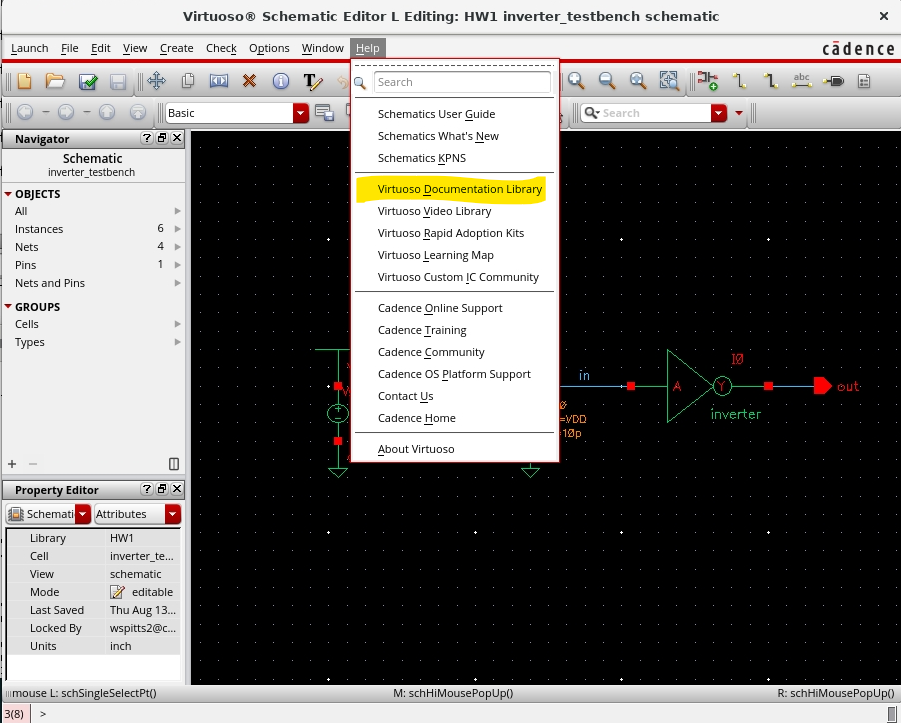
For more Information about Virtuoso
If you would like to learn more about the schematic editor, you can read through the Virtuoso Schematic Editor L User Guide that comes with the Cadence documentation. Start the documentation browser by typing
cdnshelp &
at the command prompt, and then selecting Virtuoso Schematic Editor->Virtuoso Schematic Editor L User Guide in the browser window that appears. This should display the pages that you select.
If you find that you cannot view the figures correctly in the web browser, you can browse to the documentation directory in by typing “which virtuoso” in the command line after doing the module load:
which virtuoso
/mnt/apps/public/COE/cadence_apps/IC618-270/tools/dfII/bin/virtuoso
alter the path to /mnt/apps/public/COE/cadence_apps/IC618-270/doc
where you will find PDF files for all of these documents. The cdnshelp documentation browser offers many more links for you to learn about the Cadence Design Framework.
You can also find a link to the help documents from inside Virtuoso:
Simulate the Schematic with HSPICE within Analog Artist
Set up the Simulation Environment
You are now prepared to simulate your circuit.
From the Schematic Window menu, select Launch -> ADE L. You may get another message saying that the license need to be upgraded. Simply click “Yes” or “Always” to proceed. A window will pop-up. This window is the Analog Design Environment Window.
Choose a Simulator
From the Analog Artist menu, select Setup -> Simulator/Directory/Host. Enter the fields as shown below. Choose hspiceD as your simulator. Your simulation will run in the specified Project Directory. You should default to a Project path that is not linked to ~/ (i.e. ~/hspice is not a good one). The best path for right now is in the ‘./’ directory (this will remain inside of your project space for when you ZIP Archive. You can name this anything that you want but hspice is a pretty good default.
It is worth mentioning that IF for some reason you run into quota or speed of simulation issues. You can move this to /tmp/hspice or /temp/hspice . this will cause the files to be saved on the local hard drive and reduce latency. For small projects this is not a factor and if you move from computer to computer you will not have your old simulation files if you need them. Also, if you log out they may get expunged from the system. So, this is not a good practice to default to and done more as a necessity.

Setting Up the Simulator
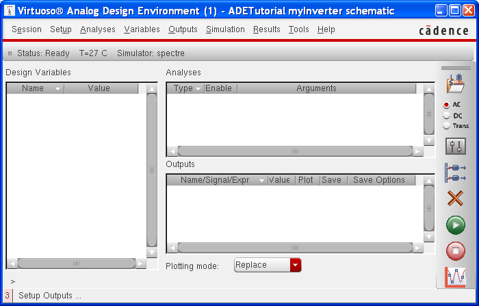
Copy the design variables into the Analog Artist (ADE L) from the CellView

Double click on the VDD_VAL or single click on the box next to it. Then, set your VDD_VAL = 0.8V (it will autocorrect this to 800m).

Set your Transient Simulation to a start of 0, stop of 40p, and a step size of 0.1p


Set your nodes to plot by selecting them on the schematic by going to Outputs -> To Be Plotted -> Select on Design . You may need to open the schematic window yourself if it does not pop up and is already open. Then click the wired nodes you want to be plotted and saved (if you click on the red squares on the end of a device or on the device itself, it will plot the current). Once you have selected what you want to select press the ESC key to stop selecting and navigate back to the ADE L window. They should now show up in the ADE L window.


Generate the HSPICE Netlist
Make sure you CHECK AND SAVE your schematics. Otherwise it will be unsuccessful in running:
     ERROR (OSSHNL-514): Netlist generation failed because of the errors reported above. The netlist might not have been generated at all, or the generated netlist could be corrupt. Fix the reported errors and regenerate the netlist.
     Loading monte.cxt
           ...unsuccessful.
So if you see the above messages check and save!
Next, generate the netlist with the following commands:
- From the ADE window menu, select Simulation -> Netlist -> Create. This will cause a window to open that displays the text of your netlist.
Saving the HSPICE Netlist
- From the ADE window menu, select Simulation -> Netlist -> Display or Simulation -> Netlist -> Create. This will cause a window to open that displays the text of your netlist.

- From the Displayed Netlist window, select File -> Save As and then save to the project directory as inv.sp
Running the HSPICE Netlist
- From the ADE window menu, select Simulation -> Netlist -> Run. This will cause a window to open that displays the text of your netlist.
You can also hit the Green button on the right that does netlist and run.
Viewing your waveform
The waveform VIVA XL (Visualization & Analysis XL) should pop up automatically with your new results. If it is already open, it might pop up behind your windows

Saving ADE L State
ADE L has the ability to load and save multiple states for simulation. This allows you to exit out of ADE L and/or Cadence and resume without having to re-setup your simulation environment and variables. You should make sure that your states are saved in the relative path ./ (this should be automatic, however if you see a ~/ or /afs/… path then these will be saved out of your project directory and therefore won’t be included in any compressed zip folders.
In the ADE L window go to Session -> Save State…

The following dialog window will appear allowing you to save multiple states for this design.

You must make sure to save your state when you make changes prior to exiting. You can save over, or create multiple different saved states. Commenting in the Description helps a lot!

Archiving the Project Folder for upload evaluation
In order to make sure that your designs are view-able by a third-party (TA, Professor, etc). You need to make sure any files that are path dependent and not in the global operating environment (the PDK directory and model files are all global paths) have a relative path extension. There are 3 important places to check:
1) ADE L Save State folder location. See the section on Saving ADE L State
2) ADE L Simulation Folder. See the section on Choose a Simulator
3) Inside of your project directory whenever you create a new Library the cds.lib file adds a absolute path link to that library. You should make sure that you go back into this file and manually edit the file path to be a relative path of ./. So, if a project is in /afs/eos/…/<username>/ECE733/homework1/Library and you are setting your design environment up in /afs/eos/…/<username>/ECE733/homework1 then you would modify the path to say ./Library. Then when you ZIP archive the homework1 project directory it will contain all of the important files.
For course work. It is good habit to create new project directories for each homework and for the project. This will keep your file submissions very clean.
You can descend into the hierarchy by going to Edit -> Hierarchy -> Descend Edit or Read. Once you select this you can click on the Symbol you want to navigate to. To Return, go to the same menu and select return. This is also how you would navigate to select internal nodes in the schematic to plot. There are also some shortcuts on the Tool Bar.

DC Simulation
(Zhao Wang)
You should note that you can set up multiple different simulations (DC, Tran, etc) in ADE L and enable or disable them.
In ADE L, select Analyses->Choose and then in the pop-out, select dc. Then click on the button of “Select Source”, and then you should click the input of the testbench, or V1 in the schematic window (which is the VPULSE source and not the VDC source). See image below with the circled source. The picture is inconsistent and will be updated later as it presently says /V0.
Then you should set up the Start, Stop and Step Size values in the dialogue. For example, here I set Start = 0, Stop = 0.800, and Step Size = 0.001. Then click OK. The image is presently low quality and will be updated later.
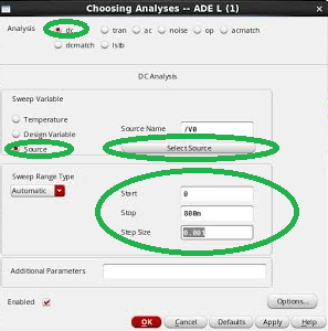

In this case, it will simulate how the V(OUT) will change as V(IN) changes from 0 to 0.8V, by sweeping the values between 0 to 0.8V of V(IN). Thus you can see the voltage transfer characteristic(VTC) of this testbench.
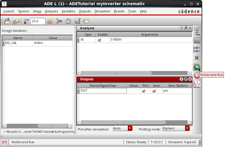
Then select Output->To Be Plotted->Select On Design, choose the line OUT to be saved and plotted. Then click on the green button(which is the short-cut of “Netlist and Run”) in ADE L, seen below.
Then the plot will be popped out, seen below.

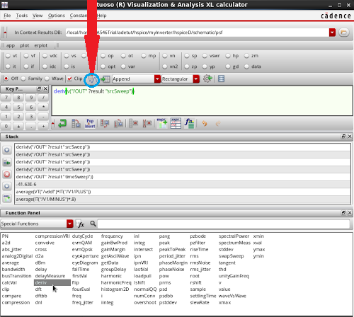
If we want to do some analyses to this waveform, we can use the calculator in the waveform window. You will notice in the figure above the /OUT waveform has been selected so it is highlighted. Next if you do Select Tools->Calculator to launch the calculator. you should be presented with the following window:

Note, you can also right click on the /OUT waveform and say SEND TO -> CALCULATOR and it will launch the calculator with the signal showing the same figure as above.
We can notice that there are a full list of functions in the calculator to be selected. For example, if we want to find VIL and VIH, we want to find where dV(OUT)/dV(IN) =-1 in the curve, then we are interested in calculating the derivative of the waveform of V(OUT). Click deriv, and then click the button circled in the picture below, to plot its derivative. Then we can see both the plots of V(OUT) and its derivative to V(IN).
Now we want to find the places where the derivative equals to -1. Here is how to put markers. First of all, select Marker->Create Marker, then a dialog will be popped out, shown below:
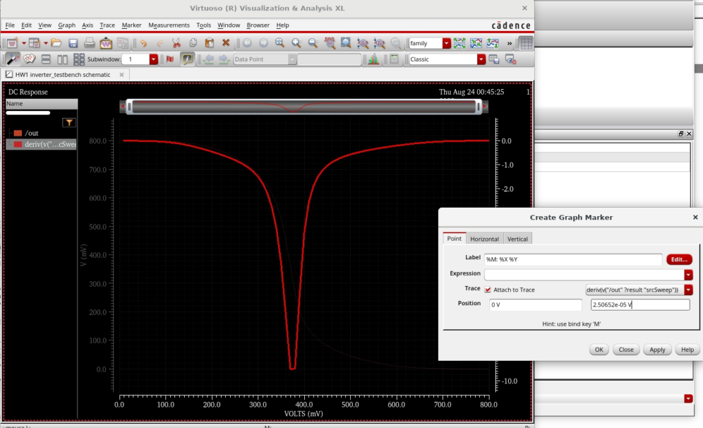
Place a marker anywhere on this curve. Next, you will need to right click on the marker and choose Point Marker Properties. Then you can select which curve to be putted on by selecting Trace option to be either /OUT, or deriv(v(“/OUT” ?result “srcSweep”)). Let’s say this time we select Trace option to be deriv(v(“/OUT” ?result “srcSweep”)). Before we click OK, we can accurately locate this marker to where we want. For example, if we want to find where the slope is -1, we can select Position option as “byYMode”, and fill in the blank as -1, shown below:
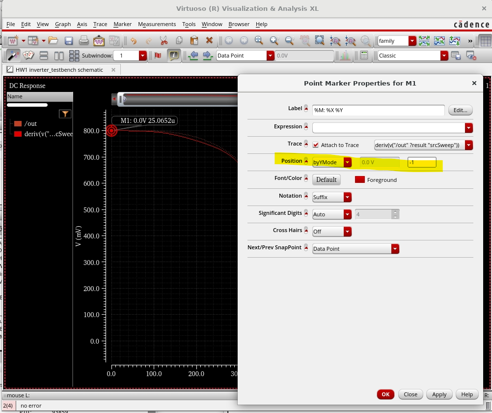
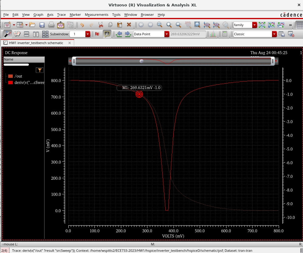
Then click OK, you can see the marker put on the waveform.
Meanwhile, you can also try to create Horizontal or Vertical markers as you have seen the tabs in the previous picture. The hot key for place single markers, horizontals or verticals are correspondingly “m”, “h”, and “v”. To edit the marker, you can double click on the marker in the waveform. Now you can have a try to explore more functions.
You can find the Virtuoso Visualization and Analysis help manuals here VIVA XL:
Also, there are other functions in the calculator that might be worth investigating. For example, the cross command can allow you to find when a particular value is crossed on the graph. So, you could solve for the crossing of where -1 is on the derivative, and then use those output to find where it crosses on the VTC curve. You can also save the calculator measurements to the ADE L setup using the gear icon:

To save your plot, you can select File->Save Image. Then just follow the instruction of the pop-out. It’s suggested that you choose your file of type as *.png or *.jpg. It’s also suggested that you enable “Replace background color with White background” in the pop-out dialogue.